Tracking a nanowire device's photocurrent responses, created by varying the wavelengths of a laser, will allow Drexel Materials researchers to make measurements and adjustments that could help them design more efficient and smaller components for smartphones, laptops and even solar panels.
A team of researchers led by Professor Jonathan Spanier and the Mesoscale Materials Laboratory has developed an innovative procedure to alleviate the challenge of measuring key features of electron behavior during the design of ever-shrinking components that allow cell phones, laptops and tablets to get increasingly thinner and more energy efficient.
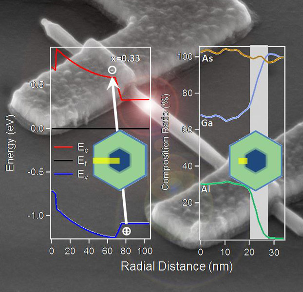
“The interface between two semiconductor materials enables most of the electronic gadgets we use each day, from computers to mobile phones, displays and solar cells,” said Ph.D. student Guannan Chen (advisor: Jonathan Spanier), lead author of the group’s report, which was recently published in Nano Letters. “One of the most important features of the interface is the height of the energy step required for the electron to climb over, known as band offset. Current methods for measuring this step height in planar devices are not practical for nanoscale devices, however, so we set off to find a better way to make this measurement.”
Measuring the band offset faced by electrons jumping from one material to another is a key component of the design process because it guides the redesign and prototyping of nanoscale components in order to make them as efficient and effective as possible.
Using laser-induced current in a nanowire device and its dependence on the wavelength of the laser, the team devised a new method to derive the band offset. As they continuously change the wavelength of the laser, they measure the photocurrent responses. From this data they are able to determine the band offset.
“Using the interface within a co-axial core-shell semiconductor nanowire as a model system, we made direct measurements of the band offset for the first time in nanowire electronics,” Chen said. “This is a significant cornerstone to freely design new nanowire devices such as solar cells, LEDs, and high speed electronics for wireless communications. This work can also extend to broader material systems which can be tailored for specific application.”
The study, which was funded primarily by the National Science Foundation, also included researchers from Lehigh University, National Research Council – Institute for Microelectronics and Microsystems (IMM-CNR) and the University of Salento in Italy, Weizmann Institute of Science and Negev Nuclear Research Center in Israel and the University of Alabama. Each group added a key component to the project.
“This remarkably simple approach to obtaining a key characteristic in individual nanowires is an exciting advance,” said Dr. Spanier, who is the lead investigator of the project. “We anticipate it will be a valuable method as we develop nanoscale electronic devices having completely new and important functionalities.”
With a better understanding of the material and electron behavior, the team will continue to pursue novel nanoscale optoelectronic devices such as new-concept transistors, electron-transfer devices and photovoltaic devices.